

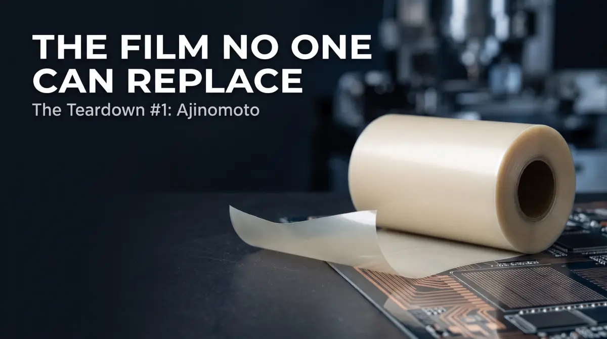
The Teardown #1: Ajinomoto · Part 1 of 3
In March 2026, a London-based activist fund made an unusual public demand of a Japanese food company: start acting like the monopolist you are.
Palliser Capital had quietly built a position among Ajinomoto Co.'s twenty-five largest shareholders, and the value-enhancement plan it published argued that the company behind the world's best-known umami seasoning is also, in the fund's phrase, the "most under-monetized AI infrastructure monopoly."
Palliser's real target was Ajinomoto Build-up Film — ABF — an epoxy-based insulating film that forms the build-up insulating layers of the advanced package substrates carrying virtually every high-performance CPU, GPU, and AI accelerator on the planet.
The arithmetic barely needed explaining. ABF represents less than 0.1% of the selling price of a GPU it makes possible. Raise that by 30% or more, Palliser argued, and no customer would notice — but shareholders would.
Ajinomoto's reply came within weeks. When Taiwanese supply-chain media reported in May that a 30% increase was coming, Ajinomoto Fine-Techno, the subsidiary that makes the film, denied it directly: no such price revision exists. In June, CEO Shigeo Nakamura said more. He told The Wall Street Journal that the company would meet demand through 2030 by expanding capacity, not by raising prices simply because it could.
That refusal is the subject of the next edition. But nothing about it can be judged until a prior question is settled: is Palliser right in the first place? Is the position as unassailable as the fund assumes?
A clarification before we begin. Nothing here is a legal monopoly. It is an overwhelming share of a very narrow category — build-up insulating films for advanced package substrates — and what keeps that share intact is the difficulty of substitution, not any regulatory barrier to entry. What this article follows is that difficulty, not the size of the share.
The 2021 Shortage Was Not a Shortage of Film
Anyone who followed the 2021 chip shortage knows part of this story already. ABF substrates — the build-up substrates that use the film — were identified then as one of the industry's hidden bottlenecks, and "the food company that makes chip materials" briefly became a favorite headline.
But the shortage was in substrate capacity, not in film. Ajinomoto was never the constraint. And almost none of that coverage explained what the material does — or why, more than twenty-five years after its 1999 launch, no material has replaced it.
A Thermosetting Film That Forms the Build-up Layers
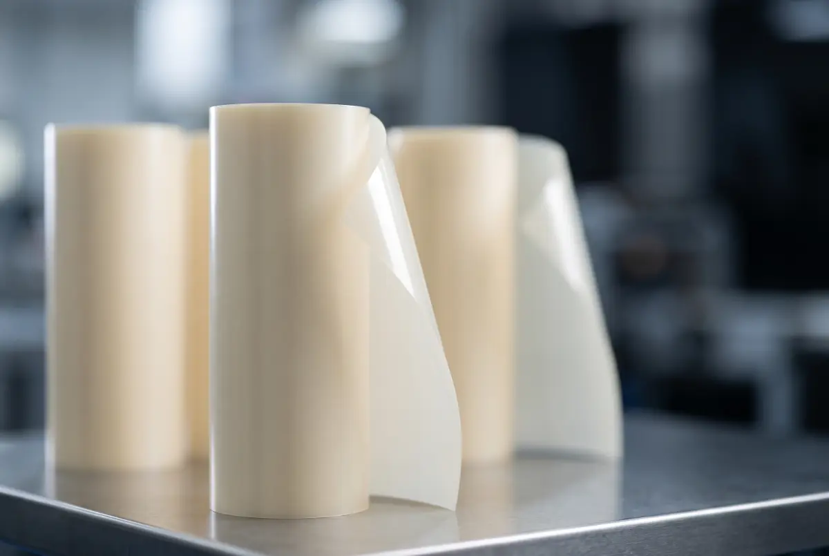
A package substrate is the foundation on which a chip is mounted, connecting circuitry measured in nanometers to a printed circuit board measured in millimeters. It is assembled as a stack — copper wiring, insulating layer, copper wiring, insulating layer — formed one level at a time. ABF is those insulating layers: a thermosetting composite of epoxy resin, hardeners, and fine inorganic fillers.
Before it arrived, insulators were applied as a liquid, screen-printed and dried one side at a time, and the results were prone to voids and uneven surfaces. The thinner and more uniform the layers had to become, the worse that method performed.
Ajinomoto approached the problem from an unlikely direction. Its electronic materials business had developed out of amino acid research, through an epoxy hardener created in the 1960s, and the formulation expertise accumulated over the decades since produced the insight that mattered: supply the insulator dry, as a film, and let the substrate maker laminate it onto the board. That meant fewer process steps and smoother surfaces — and a format suited both to laser via formation and to the semi-additive process (SAP), which forms copper wiring at micrometer scale by plating.
Four Properties That Work Against Each Other
To do that job, the film has to satisfy four demands simultaneously. Dielectric loss has to stay low enough to preserve signal integrity. The film has to expand and contract at nearly the same rate as the copper and silicon around it, or the package warps under thermal stress. Its surface has to accept a clean laser via and then roughen predictably during desmear, so that the plated copper adheres. And it has to hold that copper in place afterward — peel strength.
Individually, none of this is exotic. The difficulty is that the four demands conflict with one another.
Reduce dielectric loss and adhesion falls with it. Reduce surface roughness and peel strength falls. Add more filler to limit thermal expansion and both laser vias and fine lines become harder to form.
Each generation of ABF is a different balance among the same conflicts, and it is that accumulated body of compromise — a quarter century of it, never one headline property — that challengers have not yet reproduced.
Which is also why ABF is not a twenty-five-year-old material. It is a twenty-five-year-old position, defended by a product line reformulated for each successive node: finer fillers, lower loss, lower roughness. What maintains the moat is renewal, not inertia.
A Material Change Requires Three Stages of Qualification
This is the part that matters to anyone who evaluates supplier risk. Developing a better film and displacing ABF are two different problems, and only one of them is chemistry.
Ibiden, Shinko Electric, Unimicron — the substrate makers have adjusted their entire production flows to ABF's particular behavior: lamination parameters, laser drilling recipes, plating chemistry. A rival film therefore arrives not as a component substitution but as a change to the whole process.
Semiconductor practice requires that any such change be submitted to the customer formally and approved, with the supporting data agreed in advance and in writing. Approval proceeds in stages. The material maker qualifies with the substrate maker; the substrate maker qualifies with the chipmaker or its assembly partner; and a change this fundamental extends further, to the system maker beyond them. Every stage requires time of its own, and how much evaluation each demands varies by application.
In advanced packaging, the full sequence becomes a multi-year program carrying real yield risk — all of it carried out for a material that costs almost nothing next to the finished product.
Call it the qualification moat. The economics of a challenge are so difficult because the moat sits on the process side, not on the material side.
Rival films have been in development at electronic materials makers for many years, and Thintronics, a U.S. startup, is making a widely reported attempt, designed to be used directly in existing semi-additive lines. Development was never the obstacle. Displacement is. For build-up insulating layers in advanced package substrates, nothing has yet replaced ABF at volume, and it remains the de facto standard.
A second advantage follows from this, quieter but no less real. A supplier that has served these customers for decades hears their next requirements directly, and is frequently asked to develop products for them. A new entrant must first discover what those requirements are, and without an established relationship, specifications tend to arrive in fragments. The resulting difference in development speed is not a matter of chemistry either.
So the moat is not the patent portfolio alone, nor the formulation secrets alone. It is that an entire downstream ecosystem has been calibrated to one material, that recalibrating it is slow and expensive and risky for everyone except the incumbent, and that the incumbent is the first to learn the next requirement.
For Now, a Glass Core Still Leaves ABF in the Stack
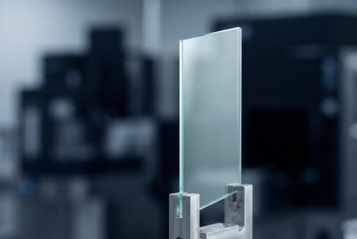
The strongest counterargument to all of this is, in technical terms, glass.
Intel committed to glass substrates in its 2023 packaging roadmap and showed a glass-core package built around its EMIB bridge technology at NEPCON Japan in January 2026, though reporting since has suggested Intel may license the technology rather than manufacture at volume itself. On timing, the company has made volume production conditional on customer commitments, and its own roadmap places that late in the decade.
Korean suppliers are moving as well. Samsung Electro-Mechanics is targeting volume production from 2027 on a pilot line in Sejong, and Absolics, an SKC subsidiary, plans limited commercial output during 2026 at a dedicated plant in Georgia. The larger packages become, the more glass's flatness and dimensional stability matter.
Two timelines are routinely confused here and need separating. TSMC's nearer-term panel-level effort, CoPoS, is scheduled by TrendForce's account for pilot production in 2027 and volume production in the second half of 2028 — but CoPoS is panel-level packaging, not a glass core. Glass-core substrates come after that, and the same analysis places commercial production beyond 2030.
The obstacles are specific rather than general. Through-glass vias tend to emerge dimensionally inconsistent and microcracked from formation, and once diameters shrink and aspect ratios rise, the limits are seed-layer uniformity and the exchange of plating solution inside the hole.
Glass does expand at close to silicon's rate, which is a large part of its appeal, but that only moves the mismatch to the organic build-up layers and copper above and below — where it still produces warpage.
Economics favor the incumbent as well. Future Market Insights puts glass substrates today at roughly two to three times the cost of their organic equivalents, with manufacturing yields of 75–85% against 90–95% for organic.
The likely shape of the transition matters more. What the industry expects is not wholesale replacement of the organic substrate but substitution of its core alone: glass in place of the resin core, organic build-up layers still formed above and below it. The glass-core substrate TSMC showed at the JPCA Show in Tokyo in June 2026 was reported to have precisely that construction. On that path, Ajinomoto's film remains in the stack.
That is the near term. There is no guarantee the configuration holds.
What Holds ABF's Moat in Place
Palliser's plan rests on several premises. The one this edition set out to test — that ABF is genuinely hard to replace — withstands that examination.
What deserves attention is where the difficulty actually lies. Formulation skill is part of it, but formulation skill alone is not what excludes challengers. What excludes them is that the cost and the risk of determining whether a rival film works fall on the substrate maker, the chipmaker, and the yield engineer — on everyone, that is, except Ajinomoto. ABF's real advantage is that testing an alternative to it is expensive for everybody else.
One condition would reverse this, and it deserves to be named. The moment what customers need exceeds what ABF can deliver, the calculation reverses: a formal evaluation opens, rival films are invited, and the winner is chosen on merit rather than on precedent. Performance is not the only possible trigger. Industrial policy aimed at domestic substitution would serve, and so would a customer deciding, on its own judgment, that a single point of failure must be eliminated.
But the moat holds for as long as good enough stays good enough.
Which leaves the question this edition has deliberately declined to answer. If the position is that strong, why does Ajinomoto not charge for it?
In the next edition: Ajinomoto could raise prices 30% tomorrow and its customers would barely notice. It refuses. We examine what that refusal actually buys, and what the most recent results reveal about whether it is working. Subscribe to receive it.
This article is an independent editorial analysis by PlaBase English and does not constitute investment advice. Company positions described here are drawn from public disclosures, company statements, and media reports as of November 2026. The technical content has been reviewed by a practitioner in semiconductor film materials.


Popular articles
China's POM Market: Inside and Outside the Tariff Barrier
27/10/2026
By Web Editorial Team
6min read

What Is an MT Ferrule? The Basics of the Ultra-Precision Part Behind AI Data Centers and Its Changing Material Requirements in the CPO Era
09/10/2026
By Web Editorial Team
25min read
The Fluoropolymer Map Just Split Three Ways. Japan Is Splitting Too.
29/09/2026
By Web Editorial Team
8min read
Japan Is Quietly Dismantling the Crackers That Built Its Plastics Industry
27/08/2026
By Web Editorial Team
6min read
Keywords
- # Bioplastic
- # Recycled plastic
- # Biodegradable plastic
- # Injection molding
- # Polypropylene
- # Polyoxymethylene
- # PPS (Polyphenylene Sulfide)
- # Polyamide
- # Plastic 3d printing
- # Moldable Plastics
- # Ocean Plastic
- # Polycarbonate
- # Cotton Plastic
- # Medical Plastic
- # Acrylonitrile Butadiene Styrene
- # Polylactic Acid
- # Comparison
- # Construction
- # Polyethylene Terephthalate
- # Automotive Plastic
